


Assembly of RF, bipolar, DMOS-, LDMOS-, GaN-transistors
СВЧ-транзисторы выпускаются в корпусах:
Package types (RF) | Can be compared with: |
КТ-4-2 | M137 (Microsemi), TO-60 (Freescale) |
КТ-44 | SOT324B (Ampleon), M156 (Microsemi), 395B-01 (Freescale) |
КТ-45 | SOT161A (Ampleon), 368-03 (Freescale) |
КТ-56 | 55JU (Microsemi), 333-04 (Freescale) |
КТ-81 | SOT324B (Ampleon), 395B-01 (Freescale) |
КТ-82 | 55KV (Microsemi) |
КТ-83 | - |
КТ-83А | - |
КТ-81С | SOT1227A (Ampleon), Style101 440166 (MACOM) |
КТ-55С-1 | SOT504A (Ampleon), SOT467C (Ampleon), 440095 (MACOM) |
КТ-103А-1 | SOT540A (Ampleon), SOT539AN (Ampleon), 375G-04 (Freescale) |
КТ-103А-2 | SOT539AN (Ampleon) |
КТ-102-1 | 368-03 (Freescale) |
КТ-57А-1 | - |
МК КТ-81А-2 | SOT502 (Ampleon) |
МК КТ-55С-3 | SOT504A (Ampleon), SOT467C (Ampleon), 440095 (MACOM) |
МК КТ-81С-2 | SOT1227A (Ampleon), Style101 440166 (MACOM) |
МК КТ-127-1 | IBK (Sumitomo) |
МК КТ-52А-1 | WF (Eudyna) |
МК КТ-44D-1 | Integra IB1261 transistor package |
МК КТ-81D-3 | Integra IB1191 transistor package |
Our existing scientific and technical experience in microelectronic design and assembling process has made it possible for to master and implement the following technologies:
Equipment:
- Gamma-188 testing machine
- EM-6520 bed-of-nails system.
Technical characteristics of the process
Key parameters measured include:
- drain to source initial current;
- drain to source remaining current;
- threshold voltage;
- drain to gate max. permissible DC voltage
Equipment:
- UMP-1 semiconductor wafer mounting systems
- EM-2075 semiconductor wafer dicing system
- EM-3027 semiconductor wafer cleaning system
- Chip picking system
Technical characteristics of the process:
- wafer diameter up to 200 mm;
- TAIKO dicing technology for ultra-thin wafers;
- wafer thickness of 100 µm to 680 µm.
- min. scribe line (kerf) width – 80 µm.
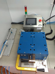
Equipment:
- Semi-automatic EM-UP-5М system
- Semi-automatic PP-5 system
- Semi-automatic TRESKY T-3202 system
- Automatic Palomar 3500 system
- Automatic Palomar 3800 system
- Automatic Palomar 3880 system
Technical characteristics of the process:
- automatic eutectic die bonding forming Au-Si (Gold-Silicon) alloy;
- bonding accuracy ± 5 µm.
- bonding up to 12 dies in a package.
Equipment:
Automatic Palomar 3880 system
Technical characteristics of the process:
- GaN-on- SiC die bonding with the help of Au-based alloys providing necessary thermal profile.
Equipment:
- Delvotec 5630 ultrasonic bonding system
- Delvotec 5632 ultrasonic deep-access bonding system
- Delvotec G5 high-capacity ultrasonic bonding system
- Delvotec G5DA high-capacity ultrasonic deep-access bonding system
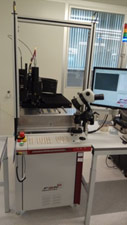
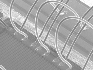
Technical characteristics of the process:
- automatic bonding of internal conductive wires with the possibility of forming stiches of the required shape using ultrasonic and thermosonic bonding methods.
- bonding with aluminum and golden wire of 17-75 µm in diameter.
- bonding accuracy 3 µm at 3σ.
- automatic control of the bonding process on-line.
Equipment:
- «Termopro» hot bench;
- ITS-500 semi-automatic sealer;
- SNOL 60/300 electric oven;
- MSH Press 6;
- Inficon UL-1000 leak tester
- Trio-tech G-254A gross leak bubble tester
Technical characteristics of the process:
- hermetic sealing of RF transistor in ceramic packages with PEK-30 adhesive (project of NIIET).
- hermetic sealing of RF transistor in ceramic packages using caps with glue.
Equipment:
- FMark-20 RL laser marking system
Technical characteristics of the process:
- ytterbium fiber laser.
- marking area 110х110 mm.
- marking speed from 1 to 4500 mm/sec.
- marking resolution - 40 µm.