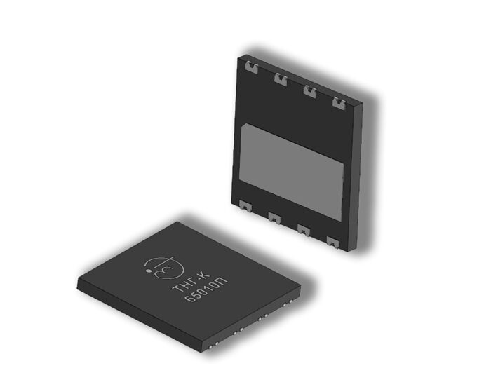
Application area: charging units for various gadgets, electric cars, electric motor control systems, systems for converting electrical energy for alternative sources (solar batteries, wind generators), power supply systems for wireless devices and spacecraft, robotics, medical devices etc.
Main parameters:
Maximum allowable drain-source voltage VDS = 650 V
Maximum direct drain current ID = 10 А
Open drain-source resistance RDS ON = 100 мОм
Maximum permissible values of electrical operation modes
Parameter | Designation | Value |
Maximum allowable direct drain-source voltage | Vds max | 650 |
Maximum direct drain current | Id max | 10 |
Maximum permissible junction temperature | Tj max | 150 |
Operating temperature range | | -55 to 150 |
Thermal resistance of junction-transistor body* | Rt j-b | 0,5 |
Electrical characteristics
Parameter | Designation | Value |
Min. | Typ. | Мах. |
Breakdown voltage drain-source | Vds max | 650 | | |
Threshold voltage | Vthr | 1 | 1.15 | 2.7 |
Gate leakage current | Ig off | | 30 | 210 |
Initial drain current | Id. in | | 57 | 170 |
Open drain-source resistance | Rds on | | 100 | |
Input capacity | C11 | | 70 | |
Output capacitance | C22 | | 20 | |
Flow-through capacity | C12 | | 2 | |
Gate Charge | QЗ | | 2.2 | |
Gate - Source Charge | Qgs | | 0,8 | |
Gate - Drain Charge | Qgd | | 0,8 | |